


5SGXEA9K2H40I2N


Or copy the link below:
- Mfr.Part #
- 5SGXEA9K2H40I2N
- Manufacturer
- Altera (Intel)
- Package / Case
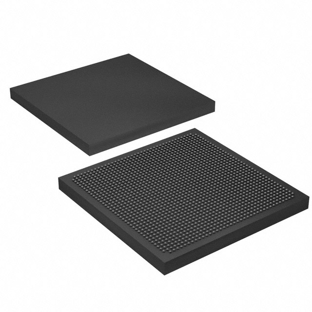
- 1517-BBGA, FCBGA
- Datasheet
- Download
- Description
- IC FPGA 696 I/O 1517HBGA
- Stock
- 35,540


- In Stock :
- 35,540
Request A Quote(RFQ)
- * Fullname:
- * Company:
- * E-Mail:
- Phone:
- Comment:
- * Quantity:
- Manufacturer :
- Altera (Intel)
- Product Category :
- FPGAs (Field Programmable Gate Array)
- Organization :
- 31700 CLBS
- Number of I/O :
- 696
- HTS Code :
- 8542.39.00.01
- Number of Logic Elements/Cells :
- 840000
- Base Part Number :
- 5SGXEA9
- Qualification Status :
- Not Qualified
- Factory Lead Time :
- 8 Weeks
- Voltage - Supply :
- 0.87V~0.93V
- Series :
- Stratix® V GX
- Total RAM Bits :
- 53248000
- Supply Voltage :
- 0.9V
- Operating Temperature :
- -40°C~100°C TJ
- RoHS Status :
- RoHS Compliant
- Number of Outputs :
- 696
- Mounting Type :
- Surface Mount
- Package / Case :
- 1517-BBGA, FCBGA
- Number of Inputs :
- 696
- Terminal Form :
- Ball
- Number of LABs/CLBs :
- 317000
- Power Supplies :
- 0.91.52.52.5/31.2/3V
- Width :
- 45mm
- Length :
- 45mm
- Packaging :
- Tray
- Height Seated (Max) :
- 3.9mm
- Surface Mount :
- yes
- Terminal Pitch :
- 1mm
- Terminal Position :
- BOTTOM
- Moisture Sensitivity Level (MSL) :
- 3 (168 Hours)
- JESD-30 Code :
- S-PBGA-B1517
- Programmable Logic Type :
- FIELD PROGRAMMABLE GATE ARRAY
- Datasheets
- 5SGXEA9K2H40I2N
FPGAs (Field Programmable Gate Array) Altera (Intel) 5SGXEA9K2H40I2N Overview
The FPGAs (Field Programmable Gate Array) Altera (Intel) 5SGXEA9K2H40I2N is a high-performance, field-programmable gate array that serves as an integral component for various advanced digital applications. Engineered by Altera, now part of Intel, this FPGA features a robust architecture that supports a wide range of uses from high-speed computing to complex digital signal processing. The 5SGXEA9K2H40I2N is built in a 1517-ball fine-pitch ball grid array (FBGA) package, making it suitable for dense board layouts and applications requiring a compact form factor but high I/O capacity, with up to 696 user I/O ports. This flexibility coupled with its powerful performance capabilities makes it an ideal choice for developers looking to push the boundaries of innovation in hardware design.
5SGXEA9K2H40I2N Features
This FPGA device integrates multiple features that cater to demanding computational needs and ensures high reliability for critical applications. Key features include its 696 I/O pins which allow for extensive interfacing capabilities, a high-density logic configuration for superior processing power, and its compatibility with Intel's state-of-the-art Quartus Prime design software. These features provide users with the flexibility to implement complex designs and accelerate product development cycles.
5SGXEA9K2H40I2N Applications
- Telecommunications Infrastructure: This FPGA can be integrated into telecommunications hardware to manage complex signal processing tasks, enhancing data transmission rates and reliability.
- Automotive Driver Assistance Systems: In automotive applications, the 5SGXEA9K2H40I2N helps manage sensor inputs and perform real-time processing for features such as collision detection and lane departure warnings.
- Medical Imaging Equipment: Utilized in medical imaging, this FPGA processes high volumes of data from imaging devices, supporting detailed and accurate image reconstruction that aids in better diagnosis.
- Industrial Automation: In industrial settings, the 5SGXEA9K2H40I2N controls machinery, processes sensor data, and automates tasks to increase efficiency and reduce human error.
- Consumer Electronics: This FPGA is used in high-end consumer electronics to enhance graphical interfaces and support complex user interfaces in smart devices.
You may place an order without registering to Chip IC. We strongly recommend that you log in before purchasing as you can track your order at any time.
RFQ (Request for Quotations)It is recommended to send RFQ to get the latest prices and stock availability about the part.Our sales will reply to your inquiry within 24 hours.
Payment MethodFor your convenience, we accept multiple payment methods in USD, Such as:PayPal, Credit Card, and wire transfer.
IMPORTANT NOTICEYou may place an order without registering to 1. You'll receive an order confirmations by e-mail soon . (Please remember to check the spam box if you didn't hear from us). 2. Since stock availability and prices may change at any time, the sales will reconfirm the order details and update you at soonest time.
Most of our products are shipped via FEDEX,DHL,UPS and SF EXPRESS...
Shipping CostShipping Cost starts at $40, but some countries will exceed $40. For example (South Africa, Brazil, India, Pakistan, Israel, etc.).If customer have shipping account, we can make shipment under customer’s shipping account with freight collect directly.
The basic freight (for package ≤0.5 KG ) depends on the time zones and countries
Once the goods are shipped, estimated delivery time depends on the shipping methods you chose. You can track it by the tracking no.
Manufacturer related products
Catalog related products


Related products
| Part | Manufacturer | Stock | Description |
|---|---|---|---|
| 5SGXAF40NAB | Altera (Intel) | 13,910 | IC FPGA 1517FBGA |
| 5SGXAF40NAC | Altera (Intel) | 10,863 | IC FPGA 1517FBGA |
| 5SGXAF40NAD | Altera (Intel) | 22,255 | IC FPGA 1517FBGA |
| 5SGXAF40NAF | Altera (Intel) | 29,605 | IC FPGA 1517FBGA |
| 5SGXAF40NAG | Altera (Intel) | 24,187 | IC FPGA 1517FBGA |
| 5SGXAF45NAA | Altera (Intel) | 27,795 | IC FPGA 1932FBGA |
| 5SGXAF45NAB | Altera (Intel) | 22,889 | IC FPGA 1932FBGA |
| 5SGXAF45NAD | Altera (Intel) | 29,429 | IC FPGA 1932FBGA |
| 5SGXAF45NAE | Altera (Intel) | 36,898 | IC FPGA 1932FBGA |
| 5SGXEA3H1F35C1G | Altera (Intel) | 1,140 | IC FPGA 432 I/O 1152FBGA |
| 5SGXEA3H1F35C1N | Altera (Intel) | 9,926 | IC FPGA 432 I/O 1152FBGA |
| 5SGXEA3H1F35C2G | Altera (Intel) | 32,695 | IC FPGA 432 I/O 1152FBGA |
| 5SGXEA3H1F35C2L | Altera (Intel) | 49,593 | IC FPGA 432 I/O 1152FBGA |
| 5SGXEA3H1F35C2LG | Altera (Intel) | 23,675 | IC FPGA 432 I/O 1152FBGA |
| 5SGXEA3H1F35C2LN | Altera (Intel) | 10,306 | IC FPGA 432 I/O 1152FBGA |
- Follow Us
-


- Payment
-


- Subscribe
- Certification
-
-


