


OR2C04A4M84-D


Or copy the link below:
- Mfr.Part #
- OR2C04A4M84-D
- Manufacturer
- Lattice Semiconductor
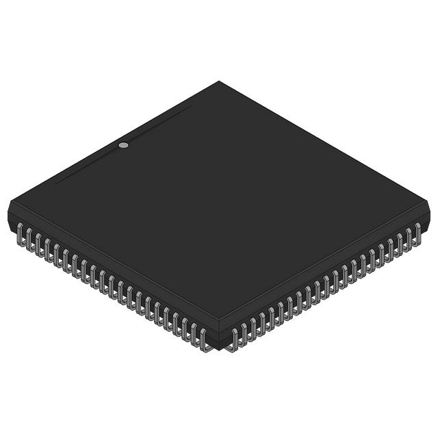
- Package / Case
- PLCC
- Datasheet
- Download
- Description
- FPGA, 100 CLBS, 4800 GATES
- Stock
- 1,001
- In Stock :
- 1,001
Request A Quote(RFQ)
- * Fullname:
- * Company:
- * E-Mail:
- Phone:
- Comment:
- * Quantity:
- Manufacturer :
- Lattice Semiconductor
- Product Category :
- FPGAs (Field Programmable Gate Array)
- Supply Voltage-Max (Vsup) :
- 5.25V
- Number of Outputs :
- 64
- Time@Peak Reflow Temperature-Max (s) :
- 30
- Number of Logic Cells :
- 400
- Peak Reflow Temperature (Cel) :
- 225
- Frequency (Max) :
- 250MHz
- Package / Case :
- PLCC
- Organization :
- 100 CLBS, 4800 GATES
- Terminal Position :
- QUAD
- Number of I/O :
- 160
- Terminal Finish :
- Tin/Lead (Sn85Pb15)
- Pin Count :
- 84
- Number of Equivalent Gates :
- 4800
- ECCN Code :
- EAR99
- Terminal Form :
- J BEND
- Max Operating Temperature :
- 70°C
- Supply Voltage :
- 5V
- JESD-30 Code :
- S-PQCC-J84
- Additional Feature :
- MAXIMUM USABLE GATES 11000
- Height Seated (Max) :
- 5.08mm
- Temperature Grade :
- COMMERCIAL
- Surface Mount :
- yes
- Programmable Logic Type :
- FIELD PROGRAMMABLE GATE ARRAY
- Moisture Sensitivity Level (MSL) :
- 3 (168 Hours)
- Number of CLBs :
- 100
- Length :
- 29.083mm
- Terminal Pitch :
- 1.27mm
- Number of Logic Blocks (LABs) :
- 400
- Number of Terminations :
- 84
- Qualification Status :
- Not Qualified
- Width :
- 29.083mm
- Combinatorial Delay of a CLB-Max :
- 2.2 ns
- Number of Inputs :
- 64
- JESD-609 Code :
- e0
- HTS Code :
- 8542.39.00.01
- Min Operating Temperature :
- 0°C
- Power Supplies :
- 5V
- RoHS Status :
- Non-RoHS Compliant
- Operating Supply Voltage :
- 3.3V
- Datasheets
- OR2C04A4M84-D
OR2C04A4M84-D Documents
FPGAs Lattice Semiconductor OR2C04A4M84-D Overview
Introducing the OR2C04A4M84-D from Lattice Semiconductor, a leading FPGA (Field Programmable Gate Array) designed to deliver exceptional performance and flexibility for a wide range of applications. This compact, highly efficient device is engineered to meet the rigorous demands of modern electronic environments. With 100 configurable logic blocks (CLBs) and 4800 gates, the OR2C04A4M84-D provides a robust platform for developers looking to optimize their systems for speed and scalability. Its small form factor and low power consumption make it an ideal choice for projects where space and energy efficiency are critical.
OR2C04A4M84-D Features
The OR2C04A4M84-D FPGA boasts several key features that make it a versatile and indispensable component in any tech developer's arsenal. With 100 CLBs and a total of 4800 gates, this device offers ample room for complex logic designs. Its optimized architecture ensures reduced power consumption and enhanced performance reliability. Additionally, the FPGA's programmability allows for rapid prototyping and easy adaptation to changing design requirements, supporting iterative development and long-term utility in diverse applications.
OR2C04A4M84-D Applications
- Consumer Electronics: This FPGA can be integrated into smart home devices and portable electronics, providing the necessary processing power and flexibility for handling complex user interfaces and connectivity tasks.
- Automotive Systems: Suitable for use in automotive applications, the OR2C04A4M84-D can manage real-time sensor data processing and actuator control, crucial for advanced driver-assistance systems (ADAS).
- Industrial Automation: In industrial settings, this FPGA helps to streamline operations by controlling machinery and processing sensor inputs rapidly, enhancing overall factory efficiency.
- Telecommunications: It plays a key role in telecommunications infrastructure by supporting signal processing operations and network management tasks essential for modern communication systems.
- Medical Devices: The OR2C04A4M84-D is also applicable in medical technology, where it processes inputs from medical imaging devices and assists in the operation of diagnostic equipment.
You may place an order without registering to Chip IC. We strongly recommend that you log in before purchasing as you can track your order at any time.
RFQ (Request for Quotations)It is recommended to send RFQ to get the latest prices and stock availability about the part.Our sales will reply to your inquiry within 24 hours.
Payment MethodFor your convenience, we accept multiple payment methods in USD, Such as:PayPal, Credit Card, and wire transfer.
IMPORTANT NOTICEYou may place an order without registering to 1. You'll receive an order confirmations by e-mail soon . (Please remember to check the spam box if you didn't hear from us). 2. Since stock availability and prices may change at any time, the sales will reconfirm the order details and update you at soonest time.
Most of our products are shipped via FEDEX,DHL,UPS and SF EXPRESS...
Shipping CostShipping Cost starts at $40, but some countries will exceed $40. For example (South Africa, Brazil, India, Pakistan, Israel, etc.).If customer have shipping account, we can make shipment under customer’s shipping account with freight collect directly.
The basic freight (for package ≤0.5 KG ) depends on the time zones and countries
Once the goods are shipped, estimated delivery time depends on the shipping methods you chose. You can track it by the tracking no.
Manufacturer related products


Catalog related products


Related products
- Follow Us
-


- Payment
-


- Subscribe
- Certification
-
-


