


5SGXEA9N3F45C2L


Or copy the link below:
- Mfr.Part #
- 5SGXEA9N3F45C2L
- Manufacturer
- Altera (Intel)
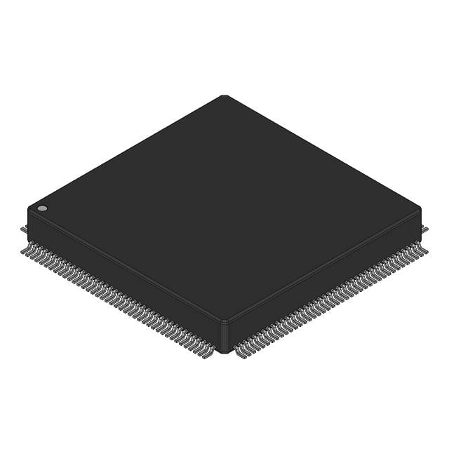
- Package / Case
- 1932-BBGA, FCBGA
- Datasheet
- Download
- Description
- IC FPGA 840 I/O 1932FBGA
- Stock
- 12,286
- In Stock :
- 12,286
Request A Quote(RFQ)
- * Fullname:
- * Company:
- * E-Mail:
- Phone:
- Comment:
- * Quantity:
- Manufacturer :
- Altera (Intel)
- Product Category :
- FPGAs (Field Programmable Gate Array)
- Mounting Type :
- Surface Mount
- Package / Case :
- 1932-BBGA, FCBGA
- Voltage - Supply :
- 0.82V~0.88V
- Total RAM Bits :
- 53248000
- Organization :
- 31700 CLBS
- Number of Inputs :
- 840
- JESD-30 Code :
- S-PBGA-B1932
- Length :
- 45mm
- Height Seated (Max) :
- 3.9mm
- Number of I/O :
- 840
- Supply Voltage :
- 0.85V
- Number of LABs/CLBs :
- 317000
- HTS Code :
- 8542.39.00.01
- Moisture Sensitivity Level (MSL) :
- 3 (168 Hours)
- Packaging :
- Tray
- Terminal Form :
- Ball
- Number of Outputs :
- 840
- Width :
- 45mm
- Factory Lead Time :
- 8 Weeks
- Operating Temperature :
- 0°C~85°C TJ
- Surface Mount :
- yes
- Power Supplies :
- 0.851.52.52.5/31.2/3V
- Base Part Number :
- 5SGXEA9
- Programmable Logic Type :
- FIELD PROGRAMMABLE GATE ARRAY
- Terminal Pitch :
- 1mm
- Qualification Status :
- Not Qualified
- Series :
- Stratix® V GX
- Number of Logic Elements/Cells :
- 840000
- RoHS Status :
- RoHS Compliant
- Terminal Position :
- BOTTOM
- Datasheets
- 5SGXEA9N3F45C2L
5SGXEA9N3F45C2L Documents

FPGAs (Field Programmable Gate Array) Altera (Intel) 5SGXEA9N3F45C2L Overview
The Altera (Intel) 5SGXEA9N3F45C2L is a high-performance integrated circuit designed for flexibility and efficiency across a broad spectrum of applications. As a core component in the field of programmable logic devices, this FPGA (Field Programmable Gate Array) facilitates rapid prototyping and innovation, allowing engineers to customize configurations to meet specific system requirements. The ability of this device to handle complex computational tasks and its reprogrammable nature makes it an indispensable tool for developers aiming to expedite product development cycles and enhance system performance.
5SGXEA9N3F45C2L Features
This model boasts an impressive array of features suited for robust digital environments, including 840 programmable I/O pins and a dense 1932FBGA package. Its design is optimized for advanced signal processing, high-speed data transfers, and substantial logic integration. These characteristics ensure that the 5SGXEA9N3F45C2L is not only capable of meeting the current demands of technological advancements but also adaptable to future innovations.
5SGXEA9N3F45C2L Applications
- Telecommunications: Utilized in infrastructure such as routers and switches, the 5SGXEA9N3F45C2L supports complex algorithms necessary for network management and data flow optimization.
- Data Centers: Critical in managing data storage and processing activities, this FPGA accelerates computing tasks, effectively reducing latency and increasing throughput in server applications.
- Automotive: Applied in driver assistance systems (ADAS), this FPGA handles real-time signal processing for sensors and cameras, enhancing vehicle safety and functionality.
- Industrial Automation: Empowers machinery with the capability to perform precise control and automation tasks, improving operational efficiency and reliability in manufacturing processes.
- Consumer Electronics: Found in devices such as high-definition televisions and gaming consoles, the FPGA enhances visual output and overall device performance through superior processing power.
You may place an order without registering to Chip IC. We strongly recommend that you log in before purchasing as you can track your order at any time.
RFQ (Request for Quotations)It is recommended to send RFQ to get the latest prices and stock availability about the part.Our sales will reply to your inquiry within 24 hours.
Payment MethodFor your convenience, we accept multiple payment methods in USD, Such as:PayPal, Credit Card, and wire transfer.
IMPORTANT NOTICEYou may place an order without registering to 1. You'll receive an order confirmations by e-mail soon . (Please remember to check the spam box if you didn't hear from us). 2. Since stock availability and prices may change at any time, the sales will reconfirm the order details and update you at soonest time.
Most of our products are shipped via FEDEX,DHL,UPS and SF EXPRESS...
Shipping CostShipping Cost starts at $40, but some countries will exceed $40. For example (South Africa, Brazil, India, Pakistan, Israel, etc.).If customer have shipping account, we can make shipment under customer’s shipping account with freight collect directly.
The basic freight (for package ≤0.5 KG ) depends on the time zones and countries
Once the goods are shipped, estimated delivery time depends on the shipping methods you chose. You can track it by the tracking no.
Manufacturer related products

Catalog related products


Related products
| Part | Manufacturer | Stock | Description |
|---|---|---|---|
| 5SGXAF40NAB | Altera (Intel) | 13,910 | IC FPGA 1517FBGA |
| 5SGXAF40NAC | Altera (Intel) | 10,863 | IC FPGA 1517FBGA |
| 5SGXAF40NAD | Altera (Intel) | 22,255 | IC FPGA 1517FBGA |
| 5SGXAF40NAF | Altera (Intel) | 29,605 | IC FPGA 1517FBGA |
| 5SGXAF40NAG | Altera (Intel) | 24,187 | IC FPGA 1517FBGA |
| 5SGXAF45NAA | Altera (Intel) | 27,795 | IC FPGA 1932FBGA |
| 5SGXAF45NAB | Altera (Intel) | 22,889 | IC FPGA 1932FBGA |
| 5SGXAF45NAD | Altera (Intel) | 29,429 | IC FPGA 1932FBGA |
| 5SGXAF45NAE | Altera (Intel) | 36,898 | IC FPGA 1932FBGA |
| 5SGXEA3H1F35C1G | Altera (Intel) | 1,140 | IC FPGA 432 I/O 1152FBGA |
| 5SGXEA3H1F35C1N | Altera (Intel) | 9,926 | IC FPGA 432 I/O 1152FBGA |
| 5SGXEA3H1F35C2G | Altera (Intel) | 32,695 | IC FPGA 432 I/O 1152FBGA |
| 5SGXEA3H1F35C2L | Altera (Intel) | 49,593 | IC FPGA 432 I/O 1152FBGA |
| 5SGXEA3H1F35C2LG | Altera (Intel) | 23,675 | IC FPGA 432 I/O 1152FBGA |
| 5SGXEA3H1F35C2LN | Altera (Intel) | 10,306 | IC FPGA 432 I/O 1152FBGA |
- Follow Us
-


- Payment
-


- Subscribe
- Certification
-
-


